Model-driven requirements engineering (MDRE) for real-time ultra-wide bandwidth signal simulation
Daniel Y. Changa,c, Neil C. Rowea, Mikhail Augustona, Man-Tak Shinga, Roberto Cristib
aSoftware Engineering, Naval Postgraduate School, Monterey, 1 University Circle, CA USA 93943;
bElectrical Engineering, Naval Postgraduate School, Monterey, 1 University Circle, CA USA 93943;
cJEWEL NAWCWD, 505 I Avenue, Suite 1, Point Mugu CA 93042-5049
ABSTRACT
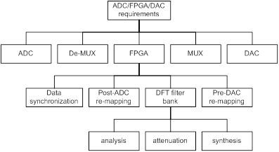
While conducting a cutting-edge research in a specific domain, we realize that (1) requirements clarity and correctness are crucial to our success, (2) hardware is hard to change, most work is in software requirements development, coding and testing [[1]], (3) requirements are constantly changing, so that configurability, reusability, scalability, adaptability, modularity and testability are important non-functional attributes, (4) if our research is successful, the results could be applied to other domains with similar problems. In this paper, we propose to use model-driven requirements engineering (MDRE) to model and guide our requirements/development, since models are easy to understand, execute, and modify. The domain for our research is Electronic Warfare (EW) real-time ultra-wide bandwidth signals simulation. The proposed four MDRE models are (1) ADC/FPGA/DAC architecture, (2) parallel data channels synchronization, (3) post-DEMUX (post-ADC) and pre-MUX (pre-DAC) bits re-mapping, and (4) Discrete Fourier Transform (DFT) filter bank.
Keywords: MDRE, requirements, real-time, ultra-wide bandwidth, ADC, DAC, FPGA, DFT filter bank
1. introduction
First, at very high level, we organize the requirements into business, feature, analysis, design, implementation and testing models. These models are briefly described in Figure 1 and Table 1 [[2]]. Then we decompose the hardware and software products into four-level hierarchical subsystems as shown in Figure 2 and Table 2 [[3]]. Lastly, we separate each subsystem requirement into functional and non-functional (such as attributes and constraints) as shown in Figure 3 and Table 3[3]. Our domain is EW real-time ultra-wide bandwidth signal simulation.
![]()
Table 1. High-level models descriptions
|
Model |
Description |
|
Business model |
EW (A-G bands) real-time ultra-wide bandwidth signal simulation |
|
Feature/goal model |
To prove that real-time ultra-wide bandwidth signals can be digitized |
|
Use case (analysis) model |
ADC � converting analog signal to digital signal |
|
De-MUX � converting serial data to parallel data |
|
|
FPGA � performing data signal processing |
|
|
MUX � converting parallel data to serial data |
|
|
DAC � converting digital signal to analog signal |
|
|
Design model |
Architecture model (described in section 4.1) |
|
Data synchronization model (described in section 4.2) |
|
|
Post-DEMUX (post-ADC) model (described in section 4.3.1) |
|
|
Pre-MUX (pre-DAC) model (described in section 4.3.2) |
|
|
DFT filter bank model (described in section 4.4) |
|
|
Implementation model |
Case study (described in section 5) |
|
Test model |
 �
�
Figure 2. Hierarchy of resulting requirements, including software and hardware
Table 2. Resulting requirements, including software and hardware
|
System |
Subsystems |
Description |
||
|
Level 1 |
Level 2 |
Level 3 |
Level 4 |
|
|
ADC/FPGA/DAC |
ADC |
|
|
See Table 1 |
|
de-MUX |
|
|
See Table 1 |
|
|
FPGA |
Post-ADC |
|
Re-map bits for DFT filter bank |
|
|
DFT filter bank |
Analysis |
Subbands division |
||
|
Attenuation (or any application) |
Simulate the effect of distance (or any application) |
|||
|
Synthesis |
Subbands combining |
|||
|
Pre-DAC |
|
Re-map bits for DAC |
||
|
MUX |
|
|
See Table 1 |
|
|
DAC |
|
|
See Table 1 |
|

Figure 3. Requirements taxonomy
Table 3. Requirements taxonomy
|
Level 1 |
Level 2 |
Level 3 |
Description |
|
Functional |
|
|
See Table 1 and Table 2 |
|
Non-functional |
Constraints |
|
0-6 GHz bandwidth, EW A-G bands |
|
�Quality |
Configurability |
configurable for wider bandwidth (H-M bands) |
|
|
Reusability |
all requirements/design models are reusable |
||
|
Scalability |
can be scaled for any number of parallel channels |
||
|
Adaptability |
can be adapted for new ADC/DAC/FPGA technologies |
||
|
Modularity |
each component is self-contained and its interface is well specified |
||
|
Testability |
provide straight through function, output=input |
||
|
Performance[1] |
Power attenuation |
none |
|
|
Noise |
low noise |
||
|
Power flatness |
constant output power across the entire frequency span |
||
|
Throughput delay |
In microseconds |
2. hypothesis
To simulate EW signals, our hypothesis is that we are able to build an efficient and scalable generic software architecture for real-time ultra-wide bandwidth signal simulation. The contributions, as well as challenges, are (1) building a generic SW/HW architecture to move data from an ADC, through an FPGA, to a DAC at an ultra-high sampling rate, (2) synchronizing� parallel data from an ultra-fast device (ADC) to a slower device (FPGA), (3) re-mapping of post-ADC and pre-DAC bits for data signal processing and digital to analog conversion, and (4) developing an efficient and scalable DFT filter bank to separate input ultra-wide bandwidth signal into multiple subbands so that each subband can be processed independently and differently. Four executable models in Table 1 for requirements/development are discussed in section 4.
3. problems/challenges
3.1 Problem/challenge 1 � SW/HW architecture for ADC/FPGA/DAC systems
As technologies advance, the ADC/DAC data sampling rate is getting faster and the number of logic cells in an FPGA is getting higher. To accommodate these rapid changes, an efficient and scalable generic SW/HW architecture is highly desirable. In addition, due to the processing speed of an ADC/DAC is much higher than an FPGA, it�s necessary to have a mechanism to de-serialize a single data stream at a higher data rate from an ADC into multiple parallel data streams at a lower data rate to an FPGA.
3.2 Problem/challenge 2 � Data synchronization problem
When moving multiple parallel data bits and sampling clocks from an ADC to an FPGA, due to different data and clock path delays, data bits at the destination device could be out of alignment. See Figure 4 for various alignment cases: (1) data is sampled correctly, (2) data is sampled at transition, and (3) data is sampled at a wrong bit.

Figure 4. Data bits misalignment
3.3 Problem/challenge 3 � Data bits re-mapping problem
The data bits in an FPGA are no longer in a sequential order after de-multiplexing (de-serializing). For example, a serial data is de-multiplexed into 4 data streams at level one as shown in Figure 5, and then each data stream is further de-multiplexed into 4 data streams at level two as shown in Figure 6. The 16 data bits after 2 levels of de-multiplexing are not usable for data signal processing. Similar situation applies to multiplexing (serializing).
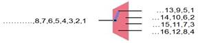
Figure 5. Level one de-multiplexing

Figure 6. Level two de-multiplexing
3.4 Problem/challenge 4 � Subband division problem
We would like to divide an ultra-wide bandwidth input signal into multiple subbands, so that each subband can be processed independently and differently. The challenges are (1) how to divide a single-channel input signal into multiple subbands, (2) how to combine multiple subbands into a single-channel output signal after processing, and (3) how to process (1) and (2) efficiently.
4. solutions/contributions/models
4.1 Solution/contribution/model 1 � building an efficient and scalable generic SW/HW architecture for ADC/FPGA/DAC system requirements/development
There are five key components in the HW architecture � (1) ADC, (2) de-multiplexer, (3) FPGA, (4) multiplexer and (5) DAC. Much attention is paid to sampling rates, data bus widths and total data throughputs. A spreadsheet is created to calculate these parameters at different components as shown in Table 4. The shaded rows are determined by users, such as the number of ADC interleaving, ADC resolution, the order of de-multiplexers, the order of multiplexers, DAC resolution and system clock. The un-shaded rows are calculated results.

Figure 7. Overall architecture
Table 4. Sampling rate, data width and throughput calculations example
|
#interleaved |
4 |
|
defined by users |
|
system clock |
12 |
GHz |
defined by users |
|
ADC clock |
3 |
GHz |
system clock / #interleaved |
|
#bytes |
4 |
|
same as #interleaved |
|
sampling rate |
12 |
bytes/sec |
ADC clock * #bytes |
|
resolution_ADC |
8 |
bits |
defined by users |
|
#bits |
32 |
bits |
#bytes * resolution |
|
throughput |
96 |
gigabits/sec |
ADC clock * #bits |
|
#demux |
4 |
|
defined by users |
|
clock_DEMUX |
0.75 |
GHz |
ADC clock / #demux |
|
#bytes_DEMUX |
16 |
bytes |
#bytes * #demux |
|
sampling rate |
12 |
bytes/sec |
clock * #bytes |
|
#bits |
128 |
bits |
#bytes * ADC resolution |
|
throughput |
96 |
gigabits/sec |
#bits * clock |
|
#demux_FPGA |
2 |
|
defined by users |
|
#bits_DSP |
256 |
bits |
#bits_DEMUX * #demux_FPGA |
|
sampling rate_FPGA |
0.375 |
GHz |
clock_DEMUX / #demux_FPGA |
|
#bytes_DSP |
32 |
bytes |
#bits_DSP / resolution |
|
#bits_DAC |
320 |
bits |
#bits_DSP * resolution_DAC / resolution_ADC |
|
#mux |
8 |
|
deinfed by users |
|
#bits mux |
40 |
bits |
#bits_DAC / #mux |
|
clock_mux |
3.000 |
GHz |
sampling rate_FPGA * #mux |
|
throughput |
120 |
gigabits/sec |
#bits_mux * clock_mux |
|
#mux_DAC |
4 |
|
deinfed by users |
|
resolution_DAC |
10 |
bits |
defined by users |
|
clock_DAC |
12 |
GHz |
same as system clock |
|
throughput |
120 |
bits/sec |
resolution_DAC * clock_DAC |
4.2 Solution/contribution/model two � data synchronization models for bits alignment requirement
We have developed three levels of algorithms for data bits alignment as requirements/development models. The first level (sampling correction) aligns the sampling clock to the center of data window for each channel. The second level (word correction) finds the number of bits being late for each channel. The third level (overall correction) moves all data bits (channels) into a FIFO by regional clocks[2], and then all data bits in the FIFO can be read by using a global clock to ensure the final data synchronization.
4.2.1 Level one � sampling correction (bit alignment) algorithm
We can align each data bit by positioning the sampling edge of the clock at the center of the data window (where data is stable) by adding delay to the datapath. A bit alignment algorithm is illustrated in Figure 8 [[4]]. Sampling correction alignment is part of initial power up calibration procedure; depending on FPGA design, it could be performed either concurrently or sequentially.
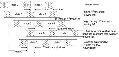
Figure 8. Level-one bits alignment procedure
Datapath delay = T(find 1st transition) + T(go through 1st transition) + T(data window) � T(half data window)
4.2.2 Level two � word correction (word alignment) algorithm
If the data rate is much faster than the clock rate, the sampled data (after level one correction) will be one or few bits late. This error can be removed if we know exactly how many bits being late. The following algorithm shows the mechanism searching for the number of bits being late by sending a test pattern.
Table 5. Level-two algorithm � word correction
|
bit_count=0; |
|
While (word<>test_pattern) { |
|
������� rotate word by one bit; |
|
������� bit count++; |
|
While_end |
The following example explains how this algorithm works. First, a training pattern �2C� (arbitrarily chosen) is sent to the data channel. If the data rate is ahead of the sampling clock by 2 bits, the received data is read as �B0� which is different from the test pattern. Applying level-two algorithm, we can obtain �2C� by rotating the 8 data bits right twice and obtain bit_count=2. We use bit_count=2 for subsequent data bit calibration.
|
2C |
2C |
2C |
|||||||||||||||||||||
|
0 |
0 |
1 |
0 |
1 |
1 |
0 |
0 |
0 |
0 |
1 |
0 |
1 |
1 |
0 |
0 |
0 |
0 |
1 |
0 |
1 |
1 |
0 |
0 |
|
1 |
0 |
1 |
1 |
0 |
0 |
0 |
0 |
clock is late by 2 bits, data=B0 |
|||||||||||||||
|
0 |
1 |
0 |
1 |
1 |
0 |
0 |
0 |
rotate right by one bit, data=58 |
|||||||||||||||
|
0 |
0 |
1 |
0 |
1 |
1 |
0 |
0 |
rotate right by one bit, data=2C |
|||||||||||||||
Figure 9. Level-two algorithm example
4.2.3 Level three � overall alignment algorithm
Once all data bits are aligned according to the sample correction and word correction algorithms, we will perform an overall alignment as listed below.
Table 6. Level-three algorithm
|
The ADC sends a training pattern to the FPGA |
|
All data bits will perform level-one (bit) and level-two (word) alignments |
|
All data bits are aligned |
|
The FPGA sends a signal to the ADC indicating training complete |
|
The ADC sends a new training pattern to the FPGA |
|
The FPGA detects the pattern change |
|
The FPGA writes data into the WRITE side of FIFO with regional clocks |
|
The output of FIFO is read with a global clock |
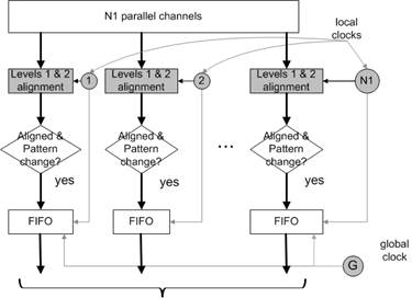
Figure 10. Level three � overall alignment algorithm
4.3 Solution/contribution 3 � Post-ADC and Pre-DAC bits re-mapping algorithms
4.3.1 Post-ADC algorithm
There are N parallel data bits from an ADC to an FPGA. If we de-multiplex each input data bit into M bits inside an FPGA, then the total number of data bits becomes N � M. Due to de-multiplexing, these N � M bits are no longer in a proper sequential order which can be processed by DSP operations; therefore, they must be re-mapped. The post-ADC algorithm for re-mapping is listed below.
Table 7. VB6 program: post-ADC algorithm
|
�N_Channel = number of subbands |
|
�demux_FPGA = 1 to demux_FPGA demultiplexer |
|
Dim bits(1 To N_Channel * demux_FPGA) As Single |
|
Dim bits_Post_ADC(1 To N_Channel * demux_FPGA) As Single |
|
For i = 1 To N_Channel Step 1 |
|
��������� For j = 1 To demux_FPGA |
|
������������������� bits_Post_ADC(i + N_Channel * (j � 1)) = bits(i * demux_FPGA � (demux_FPGA � j)) |
|
��������� Next j |
|
Next i |
|
End Sub |
Example: the actual input sequence (�15, 14, 13, 12, 11, 10, 9, 8, 7, 6, 5, 4, 3, 2, 1) is re-mapped to (�15, 11, 7, 3, 14, 10, 6, 2, 13, 9, 5, 1) by Table 7� in order to have proper ordered output bits (see Figure 11.)

Figure 11. Post-ADC re-mapping
4.3.2 Pre-DAC algorithm
After post-ADC re-mapping, we perform DSP operations and then convert data width from 8-bit to 10-bit for digital to analog conversion. Before sending data to a DAC, all data bits must be re-mapped again according to the algorithm below for similar reason as described for post-ADC re-mapping.
Table 8. VB6 program: pre-DAC algorithm
|
For i = 1 To N_DAC_bytes |
|
��������� bits2 (1 + 2 * (i � 1)) = bits1 (1 + N_DAC_RES * (i � 1)) |
|
��������� bits2 (2 + 2 * (i � 1)) = bits1 (2 + N_DAC_RES * (i � 1)) |
|
��������� bits2 ((N_DAC_bytes*2+1) + 2 * (i � 1)) = bits1 (3 + N_DAC_RES * (i � 1)) |
|
��������� bits2 ((N_DAC_bytes*2+2) + 2 * (i � 1)) = bits1 (4 + N_DAC_RES * (i � 1)) |
|
��������� bits2 ((N_DAC_bytes*4+1) + 2 * (i � 1)) = bits1 (5 + N_DAC_RES * (i � 1)) |
|
��������� bits2 ((N_DAC_bytes*4+2) + 2 * (i � 1)) = bits1 (6 + N_DAC_RES * (i � 1)) |
|
��������� bits2 ((N_DAC_bytes*6+1) + 2 * (i � 1)) = bits1 (7 + N_DAC_RES * (i � 1)) |
|
��������� bits2 ((N_DAC_bytes*6+2) + 2 * (i � 1)) = bits1 (8 + N_DAC_RES * (i � 1)) |
|
��������� bits2 ((N_DAC_bytes*8+1) + 2 * (i � 1)) = bits1 (9 + N_DAC_RES * (i � 1)) |
|
��������� bits2 ((N_DAC_bytes*8+2) + 2 * (i � 1)) = bits1 (10 + N_DAC_RES * (i � 1)) |
|
Next i |
4.4 Solution/contribution/model 4 � DFT filter bank design algorithm
DFT filter bank algorithm is an efficient way to (1) divide an ultra-wide bandwidth input signal into multiple parallel subbands (DFT analysis filter bank), (2) process subbands, and (3) combine subbands into a single data output (DFT synthesis filter bank).� DFT analysis filter bank design algorithm is shown in Table 9. DFT synthesis filter bank is the mirror image of DFT analysis filter bank.
Table 9. MATLAB program: DFT analysis filter bank design algorithm
Step 1: design a low-pass FIR filter. The order of the FIR filter is M�N, and the cutoff frequency is 1/M of overall frequency bandwidth. M is the number of channels (subbands) and N is the order for each Polyphase FIR filter. The following equation is the FIR filter design in Z-domain representation.
![]()
FIR filter Coefficients = b1, b2, � , bM�N
Step 2: re-arrange the FIR filter M�N coefficients in Polyphase format and create Polyphase FIR filters
Polyphase FIR filter coefficients:
Polyphase FIR filter #1:���� ![]()
Polyphase FIR filter #2:���� ![]()
��������������������������
Polyphase FIR filter #M:�� ![]()
Polyphase FIR filters:
![]()
![]()
��������������������������
![]()
Step 3: arrange input signal in Polyphase format
Polyphase input X(1) �������� =������������� ![]()
Polyphase input X(2) �������� =������������� ![]()
�������������������.����.
Polyphase input X(M) ������ =������������� ![]()
Step 4:
Apply Polyphase FIR filter #1 to Polyphase input #1: Y(1) = H(1)*X(1)
Apply Polyphase FIR filter #2 to Polyphase input #2: Y(2) = H(2)*X(2)
�������������������������..������.�.
Apply Polyphase FIR filter #M to Polyphase input #M:������������ Y(M) = H(M)*X(M)
Step 5:
Take FFT of Y(1), Y(2), �, Y(M)
The diagram on the left of Figure 12 shows an example of the results of 32-channel DFT analysis filter bank. In this example, the input signal is divided into 32 subbands (only 16 of them are shown since the other 16 are symmetrical.) The diagram on the right of Figure 12 shows an example of the results of 32-channel DFT synthesis filter bank. The input signal is a voice recording; the output waveform is nearly identical to the input waveform. This proves the correct re-construction of the input signal.

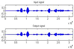
Figure 12. Results of 32-channel DFT analysis and synthesis filter banks
5. case study
Our case study is based on Tektronix DCM[3]-Digitizer/DCM-DAC/HAPS DSP single channel demo system. DCM-Digitizer is an 8-bit ADC � converting analog input signal to digital format. DCM-DAC is a 10-bit DAC � converting digital data to analog waveform. HAPS-64 has 2 Xilinx Virtex 6 FPGAs for digital signal processing.
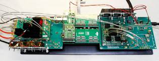
Figure 13. ADC/FPGA/DAC demo system
5.1 A GENERIC SW/HW ARCHITECTURE FOR ADC/FPGA/DAC SYSTEMS
A simplified overall architecture diagram is shown in Figure 14. Data rates, bit widths and throughputs are calculated in Table 4 (a spreadsheet program).

Figure 14. Overall architecture for our case study
5.2 Data synchronization
We generate 16,384 pseudo-random patterns to check bit accuracy across the interface from TADC-1000 to the HAPS FPGA board. The data file in the ADC analyzer is identical to the data file in the FPGA. We only show the first 10 LFSR[4] patterns in ADC and FPGA. This table proves that we were able to move data from TADC-1000 to HAPS-62 FPGA successfully by using our three alignment algorithms.
Table 10. The first 20 LFSR patterns
|
|
LFSR pattern in ADC |
LFSR pattern in FPGA |
|
File name |
usbcom_data_lfsr_16k_reference.txt |
usbcom_data_HAPS-62_lfsr_070912.txt |
|
The first 10 patterns out of 16,384 pseudo-random patterns |
FFFFFEFC01 |
FFFFFEFC01 |
|
FFFFFEFC01 |
FFFFFEFC01 |
|
|
FFFFFEFC01 |
FFFFFEFC01 |
|
|
FFFFFEFC01 |
FFFFFEFC01 |
|
|
FCFFFFFE00 |
FCFFFFFE00 |
|
|
FCFFFFFE00 |
FCFFFFFE00 |
|
|
FCFFFFFE00 |
FCFFFFFE00 |
|
|
FCFFFFFE00 |
FCFFFFFE00 |
|
|
FEFCFFFF00 |
FEFCFFFF00 |
|
|
FEFCFFFF00 |
FEFCFFFF00 |
|
|
FEFCFFFF00 |
FEFCFFFF00 |
|
|
FEFCFFFF00 |
FEFCFFFF00 |
|
|
FFFEFCFF00 |
FFFEFCFF00 |
|
|
FFFEFCFF00 |
FFFEFCFF00 |
|
|
FFFEFCFF00 |
FFFEFCFF00 |
|
|
FFFEFCFF00 |
FFFEFCFF00 |
|
|
7FFFFFFE00 |
7FFFFFFE00 |
|
|
7FFFFFFE00 |
7FFFFFFE00 |
|
|
7FFFFFFE00 |
7FFFFFFE00 |
|
|
7FFFFFFE00 |
7FFFFFFE00 |
5.3 Re-mapping
By using the re-mapping algorithms in Table 7 and Table 8, we are able to arrange bits for filtering and digital to analog conversion (see test results in section 6.)
5.4 18-tap FIR filter
We design an 18-tap FIR filter with coefficients, h[k] where k=0, 1, 2, 3� 17, and then take the convolution of h[k] and an input signal x[n] where n=0 to 31.
![]()
y[0]� = �� h[0] � x[0]������������ + h[1] � x[-1]������� + �������� + h[17] � x[-17]
y[1]� = �� h[0] � x[1]������������ + h[1] � x[0]� ������ + � ������ + h[17] � x[-16]
y[2]� = �� h[0] � x[2]������������ + h[1] � x[1]� ������ + � ������ + h[17] � x[-15]
y[3]� = �� h[0] � x[3]������������ + h[1] � x[2]� ������ + � ������ + h[17] � x[-14]
����������������������������.��..
y[30]� = h[0] � x[30] �������� + h[1] � x[29] ���� + �������� + h[17] � x[13]
y[31]� = h[0] � x[31] �������� + h[1] � x[30] ���� + � ������ + h[17] � x[14]
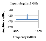
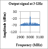
If we set h[0]=1, and the rest of coefficients to zeros, then y[n] = x[n], a pass-through condition. We can attenuate or amplify the signal by changing h[0] to a non-one value.
6. test results
The test results show that the output signal waveforms follow the input waveforms closely meeting our overall goal in Table 1, and functional and quality requirements in Table 3. Performance requirements are not addressed in this research.