

Introduction
Welcome to Lab 1! In this lab we familiarize ourselves with the FPGA and how we need to set it up so that it can be properly programmed from Simulink. The AVNET board we deal with is actually composed of a main board with the FPGA and a daughter board with Analog to Digital and Digital to Analog Converters. Therefore there are two documents relevant to this lab: the Virtex 4 FX12LC Development Board User Guide for the main board and the P160 Analog Module User Guide for the ADC/DAC board.
Problem 1 (Matlab and Simulink)
 Instructions: Open Matlab and
then Simulink. Start a new model as shown below.
Instructions: Open Matlab and
then Simulink. Start a new model as shown below.

This model just takes an input signal (say a sinusoid), digitizes it and convert it back to analog. Requirement: Simulate it with a few sinusoids and verify that you get what you expect;
Problem 2 (Simulink and Manuals)
Instructions: In this and the
next few problems we set the registers as from the
documentation.
Digital to Analog Converter (DAC1) . Double click on the DAC1 block, you see “IOB Locations” and an empty window. You need to enter data there so that the FPGA can output the data through output port 1 on the board. In the P160 Analog board you go to Table1-DAC#1 P160 Interface: look at at the JX2 P160 Connector pin numbers for MSB down to LSB. Now, with these pin numbers, go to the Table 19 P160 Connector Pin Assignments, JX2 pin numbers and find the corresponding once (‘V7’, ‘V6’ …). This is the information for DAC1: enter it in the DAC1 block;
ADC and DAC registers. Alongside the system above, make another system as shown below
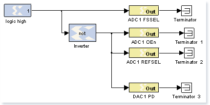
Looking at tables 1-9 in the P160 Analog Board, see the settings of these registers and set values and pin locations. For the pin locations again refer to the Table 19 P160 Connector Pin Assignments to enter the correct data. Place this in a subsystem.
Timing. Do the timing a shown and again place it in a subsystem. Your final Simulink system will be a shown below.

Problem 3 (Simulink and ISE)
Instructions: Compile it in Simulink. Exit Matlab/Simulink and compile it in ISE. This will give you the code which will then be downloaded to the FPGA board. From the video, notice that the 4 LEDs are not flashing anymore.
Problem 4 (Virtual Instrumentation)
Now we want to verify that everything works properly.
Signal Generator: try different signals (square waves, sinusoids) of different frequencies and amplitudes. The amplitudes should not exceed 1Volt.
Oscilloscope: for every signal generated, set the oscilloscope properly and look at the output signal.
Looking at the two tracks, measure 1. the time delay between the two signals, 2. the sampling interval and the sampling frequency
Problem 5 (Virtual Instrumentation)
Instructions: Set the signal generator to a sinusoid and increase the frequency until when you start seeing aliasing at the oscilloscope. Compare this frequency with the sampling frequency and verify that this is what you expect.
FPGA
Instructions: In this lab we familiarize ourselves with the FPGA and how we need to set it up so that it can be properly programmed from Simulink. The AVNET board we deal with is actually composed of a main board with the FPGA and a daughter board with Analog to Digital and Digital to Analog Converters. Therefore there are two documents relevant to this lab: the Virtex 4 FX12LC Development Board User Guide for the main board and the P160 Analog Module User Guide for the ADC/DAC board.
WebCam: Watch the webcam below to see the equipment updating live.
Oscilloscope
Instructions: In this lab we familiarize ourselves with the FPGA and how we need to set it up so that it can be properly programmed from Simulink. The AVNET board we deal with is actually composed of a main board with the FPGA and a daughter board with Analog to Digital and Digital to Analog Converters. Therefore there are two documents relevant to this lab: the Virtex 4 FX12LC Development Board User Guide for the main board and the P160 Analog Module User Guide for the ADC/DAC board.
Additional Info: In this lab we familiarize ourselves with the FPGA and how we need to set it up so that it can be properly programmed from Simulink.
Waveform Generator
Instructions: In this lab we familiarize ourselves with the FPGA and how we need to set it up so that it can be properly programmed from Simulink. The AVNET board we deal with is actually composed of a main board with the FPGA and a daughter board with Analog to Digital and Digital to Analog Converters. Therefore there are two documents relevant to this lab: the Virtex 4 FX12LC Development Board User Guide for the main board and the P160 Analog Module User Guide for the ADC/DAC board.
Help
Instructions: Watch the video below to learn about how to use the lab tools and equipment.